Note that connection labels correspond to the identifiers on the Version 1.0 schematics.
Front of Board
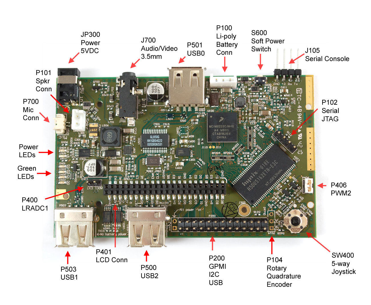
JP300
5VDC Power : Requires a regulated 5VDC power supply, positive tip, 3.5mm OD, 1.4mm ID barrel jack (aka a 3.8mm or 4mm connector).
Schematics indicate 2A peak. According to AdaFruit the power draw for the subsystems is roughly:
- 300 mA for the base hardware (processor, RAM, SD card),
- 200 mA for the USB hub (not including power to the USB devices),
- 300 mA for a speaker plugged into the 2W output,
- 500 mA max for charging a Lipoly battery.
P100
Li-poly battery connector : JST B3B-EH-A connector.
If powering from a Li-poly, USB0 will be powered, 1 and 2 will not.
There is a fourth USB connection on the GPIO header which is
also powered by the Li-poly boost system.
ref
P102
Serial JTAG header - 0.1” male header (DNP)
- Pin 1 : 3.3v
- Pin 2 : DEBUG
- Pin 3 : PSWITCH
- Pin 4 : GND
P104
Rotary Quadrature Encoder (no connector, solder points only)
- Pin 1 : ROTARYA
- Pin 2 : GND
- Pin 3 : ROTARYB
P200
9x2 header : USB, I2C and GPMI
The following signals are available (by pin number)
Bottom Row, Left to Right
- 1 - 5V
- 3 - USBC1 N
- 5 - USBC1 P
- 7 - GND
- 9 - Vid to Ext
- 10 - i2C SCL
- 11 - i2C SDA
- 15 - 3.3V
- 17 - LCD XP
- 19 - LCD YP
- 21 - LCD XM
- 23 - LCD YM
- 25 - HOST TO CP UART
Top Row, Left to Right
- 2 - GPMI D00
- 4 - GPMI D01
- 6 - GPMI D02
- 8 - GPMI D03
- 10 - GPMI D04
- 12 - GPMI D05
- 14 - GPMI D07
- 16 - GPMI D06
- 18 - OSC TO FM
- 20 - PWM2
- 22 - CHUMBY BEND
- 26 - CP TO HOST UART
P400
LRADC1 : Low Resolution Analog to Digital Converter
- Pin 1 : LRADC1 (CPU)
- Pin 2 : connected to pin 39 of P401 (why?)
P401
22x2 Header, LCD Connector
Top Row, Right to Left
- 1 : GND
- 3 : LCD T B1
- 5 : LCD T B3
- 7 : LCD T B5
- 9 : LCD T G0
- 11 : LCD T G2
- 13 : LCD T G4
- 15 : GND
- 17 : LCD T R1
- 19 : LCD T R3
- 21 : LCD T R5
- 23 : LCD VSYNC T
- 25 : LCD DOTCLK
- 27 : LCD ENABLE T
- 29 : LED A
- 31 : LCD WR E
- 33 : LCD CS
- 35 : LINE1 INL
- 37 : GND
- 39 : LRADC1 EXT
- 41 : LCD XP
- 43 : LCD XM
Bottom Row, Right to Left
- 2 : LCD T B0
- 4 : LCD T B2
- 6 : LCD T B4
- 8 : GND
- 10 : LCD T G1
- 12 : LCD T G3
- 14 : LCD T G5
- 16 : LCD T R0
- 18 : LCD T R2
- 20 : LCD T R4
- 22 : P 3.3V
- 24 : LCD HSYNC T
- 26 : GND
- 28 : LCD RESET
- 30 : LED K
- 32 : LCD RS
- 34 : LCD DET
- 36 : LINE1 INR
- 38 : VDDA
- 40 : LRADC0
- 42 : LCD YP
- 44 : LCD YM
P406
PWM2 : Pulse Width Modulation
- Pin 1 : GND
- Pin 2 : PWM2 (CPU)
P500
USB2 : USB Type A Female
P503
USB1 : USB Type A Female (is this really USB4?)
Note that the power to this port (and P500?) is software controlled and may be off at power-up. It can be enabled as explained here.
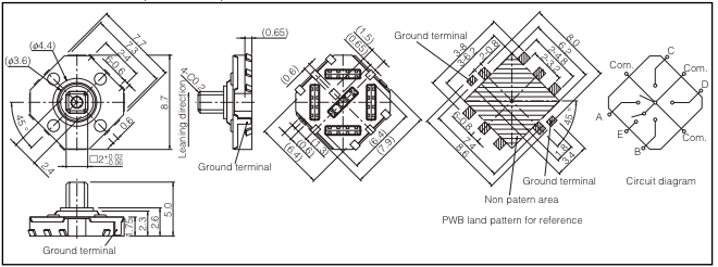
SW400
DPad switch type EVQQ7. The Data sheet is available. Sample code is available.
- A : GPMI CE0n : BANK2_PIN28
- B : GPMI WPn : BANK0_PIN23
- C : GPMI WRn : BANK0_PIN24
- D : GPMI RDn : BANK0_PIN25
- E : PWM4 : BANK_1_PIN30 (aka CHUMBY BEND)

Accelerometer
A Freescale MMA7455L 3-axis accelerometer with adjustable sensitivity from +-2G to +-8G is accessible over I2C at device address 0x1D.
The Datasheet is available, sample code is available.

Green LEDs
The 4 green LEDs are connected to the following GPIO pins:
- GPMI_D00
- GPMI_D01
- GPMI_D02
- GPMI_D03
Importantly, before any of the LEDs can be used, the transistor on GPMI_RDY0 must be turned on to ground the LEDs.
Sample code is available.
